Ticker : 300236.SZ
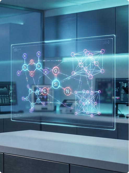
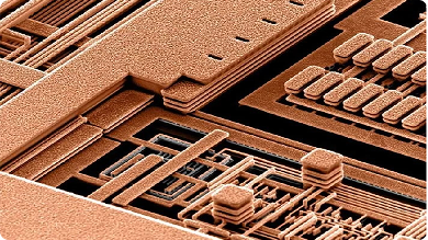
Copper interconnects are the "neural networks" of modern chips. Like microscopic wires, they are responsible for transmitting electrical signals between billions of transistors and serve as the lifeline of information flow. Their excellent electrical conductivity and low-power characteristics are the key to enabling chips to achieve high speed, high performance and small size.
MoreCleaning solutions are a series of key chemical reagents used to remove contaminants from the surface of wafers during the chip manufacturing process. Their purity, performance and stability directly determine the yield and reliability of semiconductor devices.
MoreEtchant is a key material in the wet etching process of chips. With hydrofluoric acid, nitric acid and other substances as the main components, it achieves precision etching through redox reactions and is widely used in chip manufacturing.
MorePhotoresist is the core photosensitive material of the lithography process. Through coating, exposure and development, it accurately transfers the circuit design on the photomask onto the wafer surface, forming a pattern barrier for subsequent etching or ion implantation.
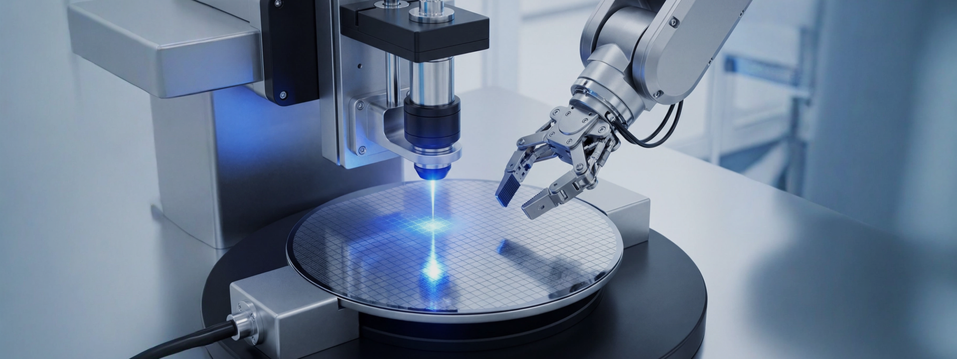
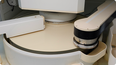
MoreChemical Mechanical Polishing (CMP) planarizes silicon wafers or other substrate materials during processing using chemical etching and mechanical force. Integrated circuits generally adopt multi‑layer three‑dimensional wiring, requiring repeated cycles in front‑end manufacturing. CMP is a key process for wafer planarization and an important step in advancing process technology nodes.
MoreMore
More
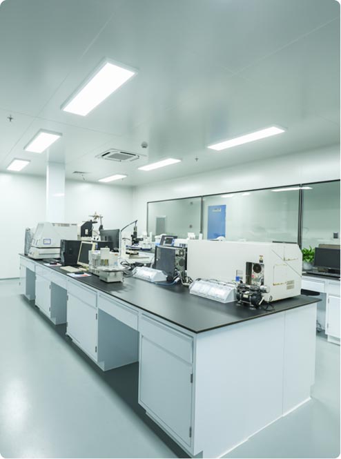
Lead frame plating and cleaning equipment are core for traditional packaging. They remove contaminants and form uniform metal coatings to improve conductivity and reliability. Advanced packaging wafer wet processing equipment works with electronic chemicals for photoresist stripping, developing, etching, cleaning, plating, etc. Modular design supports Bump, TSV and RDL processes.
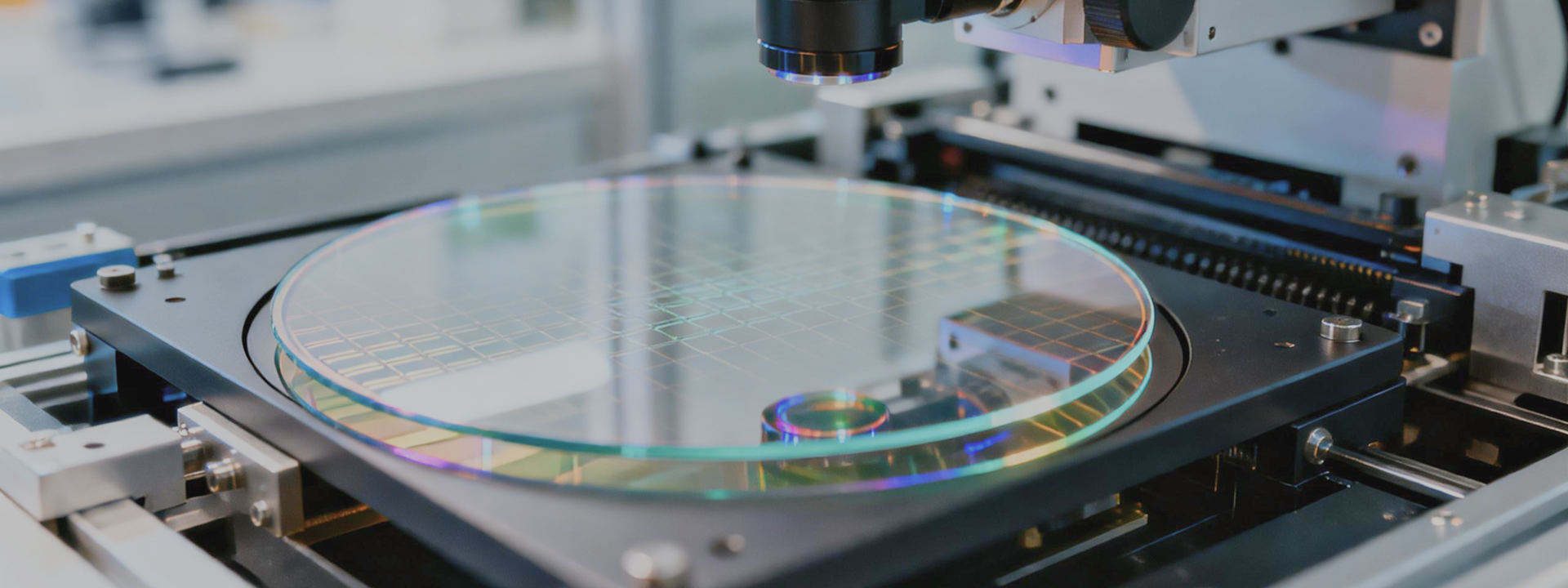
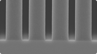
MoreThe dicing blade is the core tool for precision cutting of wafers into individual chip units. For chips of different materials and processes, it is necessary to accurately match dicing blades of different specifications to ensure cutting quality and chip yield.
MoreWe focus on national semiconductor needs and global cutting-edge IC materials.
We insist on independent R&D and innovation to achieve self-controlled high-end IC technologies.
We focus on national semiconductor needs and global cutting-edge IC materials. We insist on independent R&D and innovation to achieve self-controlled high-end IC technologies.
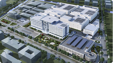
•Overview of the 50,000-ton IC Key Process Materials Project, Headquarters & R&D Center in Songjiang, Shanghai

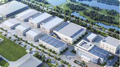
•Phase I of 2nd Production Base in Hefei, Anhui successfully launched.
•Company’s 5th core technology — Electronic Etching Technology officially released.
•Project Initiation & Planning of the Production Base in Shanghai Chemical Industry Park
•Initiated the R&D project of polishing slurry for wafer manufacturing, establishing the fourth core technology direction
•Initiated the R&D project of photoresist for wafer manufacturing, officially laying out the third core technology — photoresist
•The company developed its second-generation core technologies for electronic electroplating and electronic cleaning, with its technological strength continuously enhanced
•In June, the company was successfully listed on the ChiNext Board of the Shenzhen Stock Exchange (Stock Code: 300236)
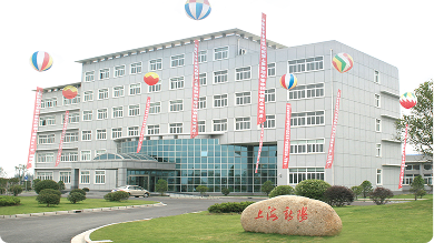
•The company’s new plant in Songjiang was completed and put into operation, marking a new stage in production capacity and R&D capabilities.
•The first-generation core technologies for electronic electroplating and electronic cleaning were developed, laying the foundation for a relatively complete technical system and product portfolio.
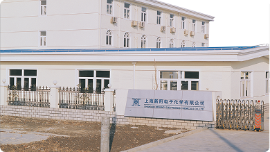
•The company acquired land and built a factory in Jiangqiao Town, Jiading District, Shanghai, owning its first proprietary production base.
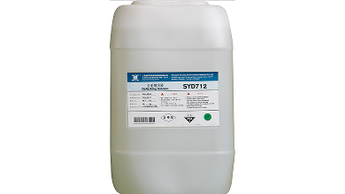
•The company’s first product—defalshing solution SYD712—was successfully launched onto the market, marking its official entry into the semiconductor packaging field.
•In July, Shanghai Sinyang Chemical Co., Ltd. was established, kicking off its entrepreneurial journey.